

Introduction
Today Electronics is unavoidable! It dominates our lives in many ways and you can’t deny it. Physics and technology improvements and advancements have created a world which relies on electronic services and communication. Nowadays, it is common to own numerous electronic devices for one reason or another. All of them have a purpose and many of them seem quite necessary in day to day lives of people.One of the most popular and most important electronic today is the cell phone. It seems like everyone has a cell phone; even young children are becoming owners of their very own cell phones! Yes, maybe you can deny this with reference to poor countries. But we all know that cell phones are an extremely popular form of communication and are relied upon by families, businesses, friends, and pretty much anyone who needs to talk on the phone.
Electronics which might be even more important, though most likely less owned, are computers. So much communication is done online today, that it is vital for many people to own computers. Universities now expect all of their students to own their own computers, because so many assignments, lectures, and information is given and received online.
Today Electronics is unavoidable! It dominates our lives in many ways and you can’t deny it. Physics and technology improvements and advancements have created a world which relies on electronic services and communication. Nowadays, it is common to own numerous electronic devices for one reason or another. All of them have a purpose and many of them seem quite necessary in day to day lives of people.One of the most popular and most important electronic today is the cell phone. It seems like everyone has a cell phone; even young children are becoming owners of their very own cell phones! Yes, maybe you can deny this with reference to poor countries. But we all know that cell phones are an extremely popular form of communication and are relied upon by families, businesses, friends, and pretty much anyone who needs to talk on the phone.
Definition of Electronics!
Electronics is the branch of science that is
concerned with the study of flow and control of electrons and the study of
their behavior and effects in conductors, semiconductors and insulators, and
with devices using such electrons. This control of electrons is accomplished by
devices that resist, carry, select, steer, switch, store, manipulate, and
exploit the electron.

Semiconductors
The Concept of Energy Band in Solids
In solid-state physics, the electronic
band structure (or simply band structure) of a
solid describes those ranges of energy that an electron within the solid may
have (called energy bands, allowed bands, or simply bands) and ranges of energy that it may not have
(called band gaps or forbidden bands).
Band theory derives
these bands and band gaps by examining the allowed quantum mechanical wave
functions for an electron in a large, periodic lattice of atoms or molecules.
Band theory has been successfully used to explain many physical properties of
solids, such as electrical resistivity and optical absorption, and forms the
foundation of the understanding of all solid-state devices (transistors, solar
cells, etc.).
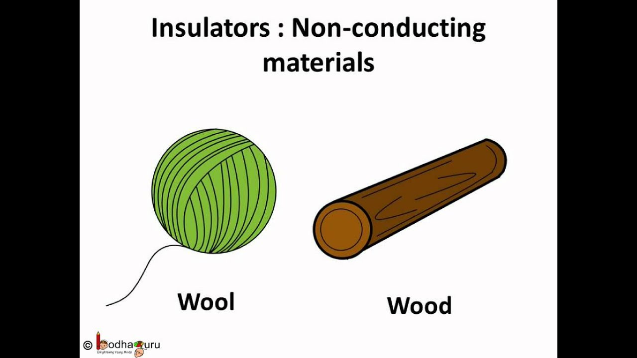
Insulators
An electrical insulator is
a material whose internal electric charges do not flow freely, and therefore
make it impossible to conduct an electric current under the influence of an
electric field. This contrasts with other materials, semiconductors and
conductors, which conduct electric current more easily.
The property that distinguishes an insulator is its
resistivity; insulators have higher resistivity than semiconductors or
conductors.
A perfect insulator does not exist, because even insulators
contain small numbers of mobile charges (charge carriers) which can carry
current. In addition, all insulators become electrically conductive when a
sufficiently large voltage is applied that the electric field tears electrons
away from the atoms. This is known as the breakdown voltage of an insulator.
Some materials such as glass, paper and Teflon, which have
high resistivity, are very good electrical insulators. A much larger class of
materials, even though they may have lower bulk resistivity, are still good enough to prevent significant current from flowing
at normally used voltages, and thus are employed as insulation for electrical
wiring and cables. Examples include rubber-like polymers and most plastics.
A conductor is an
object or type of material that allows the flow of electrical current in one or
more directions. For example, a wire is an electrical conductor that can carry
electricity along its length.
In metals such as copper or aluminum, the movable charged
particles are electrons. Positive charges may also be mobile, such as the cationic
electrolyte(s) of a battery, or the mobile protons of the proton conductor of a
fuel cell. Insulators are non-conducting materials with few mobile charges and
support only insignificant electric currents.
Semiconductors


A semiconductor material
has an electrical conductivity value falling between that of a conductor, such
as copper, and an insulator, such as glass. Semiconductors are the foundation
of modern electronics. Semiconducting materials exist in two types: elemental materials and compound materials.
The modern understanding of the properties of a
semiconductor relies on quantum physics to explain the movement of electrons
and holes in a crystal lattice. The unique arrangement of the crystal lattice
makes silicon and germanium the most commonly used elements in the preparation
of semiconducting materials.
An increased knowledge of semiconductor materials and
fabrication processes has made possible continuing increases in the complexity
and speed of microprocessors and memory devices. Some of the information on
this page may be outdated within a year because new discoveries are made in the
field frequently.
Examples of semiconductors are Silicon, Germanium.

The effect of temperature on the conductivity
of conductors, semiconductors and insulators.
The conductivity of pure defect free metal decreases with
increase in temperature. With increased temperature in a metal, thermal energy
causes atoms in metal to vibrate, in this excited state atoms interact with and
scatter electrons.
Thus decreasing the mean free path, and hence the mobility
of electrons too decreases, and resistivity increases (resistivity =
1/conductivity).
The electrical conductivity of a semiconductor will increase
exponentially with an increase in temperature, as temperature increases the
electrons in the valance band will gain energy and go into the higher energy
levels in the conduction band where they become charge carriers.
The increase in conduction can also be explained, I
guess,due to the formation of Cooper pairs and hence the creation of Phonon
field.
Types of Semiconductors
There are two types of semiconductors
i.
Intrinsic semiconductors
ii.
Extrinsic semiconductors
Intrinsic semiconductors
An intrinsic semiconductor material is chemically very pure
and possesses poor conductivity. It has equal numbers of negative carriers
(electrons) and positive carriers (holes). Examples are Silicon and Germanium.
A silicon crystal is different from an insulator because at
any temperature above absolute zero temperature, there is a finite probability
that an electron in the lattice will be knocked loose from its position,
leaving behind an electron deficiency called a "hole."
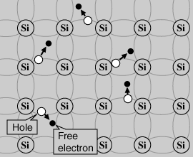 If a voltage is applied, then both the electron and the hole
can contribute to a small current flow. The conductivity of a semiconductor can
be modeled in terms of the band theory of solids.
If a voltage is applied, then both the electron and the hole
can contribute to a small current flow. The conductivity of a semiconductor can
be modeled in terms of the band theory of solids.
The band model of a semiconductor suggests that at ordinary
temperatures there is a finite possibility that electrons can reach the
conduction band and contribute to electrical conduction. The term intrinsic
here distinguishes between the properties of pure "intrinsic" silicon
and the dramatically different properties of doped n-type or p-type
semiconductors.
The current flow in an intrinsic semiconductor is influenced
by the density of energy states which in turn influences the electron density
in the conduction band. This current is highly temperature dependent. The
electrical conductivity of intrinsic semiconductors increase with increasing
temperature.
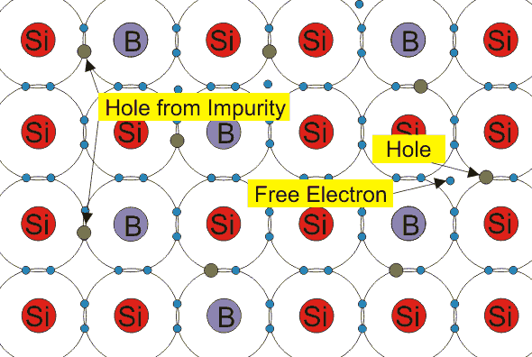
Extrinsic
semiconductors
Extrinsic semiconductor is an improved intrinsic
semiconductor with a small amount of impurities added by a process,known as
doping, which alters the electrical properties of the semiconductor and
improves its conductivity.
Introducing impurities into the semiconductor materials (doping process) can control their conductivity.Doping
process produces two groups of semiconductors:
i.
The negative charge conductor (n-type).
ii.
The positive charge conductor (p-type).
Semiconductors are available as either elements or
compounds. Silicon and Germanium are the most common elemental semiconductors.
Compound Semiconductors include InSb, InAs, GaP, GaSb, GaAs, SiC, GaN. Si and
Geboth have a crystalline structure called the diamond lattice. That is, each
atom has its four nearest neighbors at the corners of a regular tetrahedron
with the atom itself being at the center.
In addition to the pure element semiconductors, many alloys
and compounds are semiconductors. The advantage of compound semiconductor is
that they provide the device engineer with a wide range of energy gapsand
mobilities, so that materials are available with properties that meet specific
requirements. Some of these semiconductors are therefore called wide band gap
semiconductors.
The Mechanism of Doping Intrinsic Semiconductors
Describe the mechanism of doping intrinsic semiconductors
The addition of a small percentage of foreign atoms in the
regular crystal lattice of silicon or germanium produces dramatic changes in
their electrical properties, producing n-type and p-type semiconductors.
Pentavalent impurities
The addition of pentavalent impurities such as
antimony,arsenic or phosphorous contributes free electrons, greatly increasing
the conductivity of the intrinsic semiconductor. Phosphorous may be added by
diffusion of phosphine gas (PH3).(5 valence electrons) produce n-type
semiconductors by contributing extra electrons.
Trivalent impurities
(3 valence electrons) produce p-type semiconductors by
producing a "hole" or electron deficiency.
N-Type Semiconductor
The addition of pentavalent impurities such as antimony, arsenic
or phosphorous contributes free electrons,greatly increasing the conductivity
of the intrinsic semiconductor. Phosphorous may be added by diffusion
ofphosphine gas (PH3).
P-Type Semiconductor
The addition of trivalent impurities such as boron, aluminum
or gallium to an intrinsic semiconductor creates deficiencies of valence
electrons,called "holes". It is typical to use B2H6diborane gas to
diffuse boron into the silicon material.
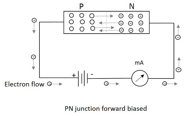
P-n
junctions
P-n
junctions are formed by joining n-type
and p-type semiconductor materials.
Since the n-type region has a high electron concentration
and the p type a high hole concentration, electrons diffuse from the n-type
side to the p-type side. Similarly, holes flow by diffusion from the p-type side to the n-type side.
If the electrons and holes were not charged, this diffusion
process would continue until the concentration of electrons and holes on the
two sides were the same, as happens if two gasses come into contact with each
other. However, in a p-n junction,
when the electrons and holes move to the other side of the junction, they leave
behind exposed charges on dopant atom sites, which are fixed in the crystal
lattice and are unable to move.
On the n-type side,
positive ion cores are exposed. On the p-type side,
negative ion cores are exposed. An electric field Ê forms between the positive
ion cores in the n-type material and negative ion
cores in the p-type material. This region is
called the "depletion region" since the electric field quickly sweeps
free carriers out, hence the region is depleted of free carriers.
Diodes
A semiconductor diode is
a crystalline piece of semiconductor material with a p–n junction connected to
two electrical terminals. In electronics, a diode is a
two-terminal electronic component with asymmetric conductance; it has low
(ideally zero) resistance to current in one direction, and high (ideally
infinite) resistance in the other
The
Construction of P-N Junction
When the polarity of the battery is such that electrons are
allowed to flow through the diode, the diode is said to be forward-biased. Conversely, when the battery is
“backward” and the diode blocks current, the diode is said to be reverse-biased. A diode may be thought of as like a
switch: “closed” when forward-biased and “open” when reverse-biased.
Diode behavior is analogous to the behavior of a hydraulic
device called a check valve. A check valve allows
fluid flow through it in only one direction.

The Mode of Action a P-N Junction
In a p-n junction, electrons cross over the boundary from
the n-type material to holes in the p-type material. At the same time, holes
cross over from the p-side to the n-side and capture electrons. This movement
of holes and electrons causes the n-side to become positively charged and the
p-side to become negatively charged. A p.d is created across the junction to
stop further electron flow.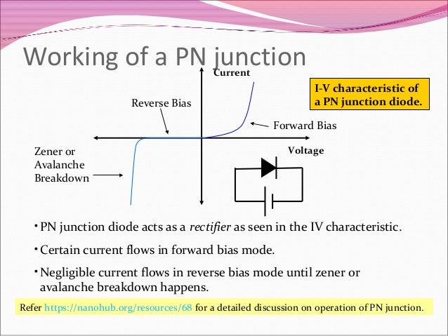
The Types of Diodes

Backward
diode: This type of diode is
sometimes also called the back diode. Although not widely used, it is a form of
PN junction diode that is very similar to the tunnel diode in its operation. It
finds a few specialist applications where its particular properties can be
used. Read more about the Backward diode.
BARITT diode: This form of diode gains its name from the words
Barrier Injection Transit Time diode. It is used in microwave applications and
bears many similarities to the more widely used IMPATT diode.
Gunn Diode:Although not a diode in the form of a PN junction, this type
of diode is a semiconductor device that has two terminals. It is generally used
for generating microwave signals.
Laser diode:This type of diode is not the same as the ordinary light
emitting diode because it produces coherent light. Laser diodes are widely used
in many applications from DVD and CD drives to laser light pointers for
presentations. Although laser diodes are much cheaper than other forms of laser
generator, they are considerably more expensive than LEDs. They also have a
limited life.
Light emitting diodes: The light emitting diode or LED is one of the most popular
types of diode. When forward biased with current flowing through the junction,
light is produced. The diodes use components miconductors, and can produce a
variety of colours, although the original colour was red. There are also very
many new LED developments that are changing the way displays can be used and
manufactured. High output LEDs and OLEDs are two examples.


Photodiode:The photo-diode is used for detecting light. It is found
that when light strikes a PN junction it can create electrons and holes.
Typically photo-diodes are operated under reverse bias conditions where even
small amounts of current flow resulting from the light can be easily detected.
Photo-diodes can also be used to generate electricity. For some applications,
PIN diodes work very well as photodetectors.
PIN diode:This type of diode is typified by its construction. It has
the standard P type and N-type areas, but between them there is an area of
Intrinsic semiconductor which has no doping. The area of the intrinsicse
miconductor has the effect of increasing the area of the depletion region which
can be useful for switching applications as well as for use in photodiodes,
etc.
PN Junction: The standard PN junction may be thought of as the
normal or standard type of diode in use today. These diodes can come as small
signal types for use in radio frequency, or other low current applications
which may be termed as signal diodes. Other types may be intended for high
current and high voltage applications and are normally termed rectifier diodes.
Schottky diodes:This type of diode has a lower forward voltage drop than
ordinary silicon PN junction diodes. At low currents the drop may be somewhere
between 0.15 and 0.4 volts as opposed to 0.6 volts for a silicon diode. To
achieve this performance they are constructed in a different way to normal
diodes having a metal to semiconductor contact. They are widely used as
clamping diodes, in RF applications, and also for rectifier applications.
Step recovery diode:A form of microwave diode used for generating and shaping
pulses at very high frequencies. These diodes rely on a very fast turn off
characteristic of the diode for their operation.
Tunnel diode:Although not widely used today, the tunnel diode was used
for microwave applications where its performance exceeded that of other devices
of the day.
Varactor diode or varicap
diode:This type of diode is used in many
radio frequency (RF) applications. The diode has a reverse bias placed upon it
and this varies the width of the depletion layer according to thevoltage placed
across the diode. In this configuration the varactor or varicap diode acts like
a capacitor with the depletion region being the insulating dielectric and the
capacitor plates formed by the extent of the conduction regions. The
capacitance can be varied by changing the bias on the diode as this will vary
the width of the depletion region which will accordingly change the
capacitance.
Zener diode:The Zener diode is a very useful type of diode as it
provides a stable reference voltage. As a result it is used in vast quantities.
It is run under reverse bias conditions and it is found that when a certain
voltage is reached it breaks down. If the current is limited through a
resistor, it enables a stable voltage to be produced. This type of diode is
therefore widely used to provide a reference voltage in power supplies. Two
types of reverse breakdown are apparent in these diodes: Zener breakdown and
Impact Ionisation. However the name Zener diode is used for the reference
diodes regardless of the form of breakdown that is employed.
The Construction of a Half-wave and Full-Wave Rectifier
A rectifier is an
electrical device that converts alternating current (AC), which periodically
reverses direction,to direct current (DC), which flows in only one direction.
The process is known as rectification.
In a half-wave rectifier circuit, a
load resistance is connected in series with the PN junction diode. Alternating
current is the input of the half wave rectifier. It is nothing
more than a single pn junction diode connected in series to the load resistor.
It consists a step down transformer, a diode connected to
the transformer and a load resistance connected to the cathode end of the
diode. The circuit diagram of half wave transformer is shown below:
The main supply voltage is given to the transformer which
will increase or decrease the voltage and give to the diode. In most of the
cases we will decrease the supply voltage by using the step down transformer
here also the output of the step down transformer will be in AC. This decreased
AC voltage is given to the diode which is connected serial to the secondary
winding of the transformer, diode is electronic component which will allow only
the forward bias current and will not allow the reverse bias current. From the
diode we will get the pulsating DC and give to the load resistance RL.
Working of Half Wave Rectifier:
The input given to the rectifier will have both positive and
negative cycles. The half rectifier will allow only the positive half cycles
and omit the negative half cycles. So first we will see how half wave rectifier
works in the positive half cycles.
Positive Half Cycle:
- In
the positive half cycles when the input AC power is given to the primary
winding of the step down transformer, we will get the decreased voltage at
the secondary winding which is given to the diode.
- The
diode will allow current flowing in clock wise direction from anode to
cathode in the forward bias (diode conduction will take place in forward
bias) which will generate only the positive half cycle of the AC.
- The
diode will eliminate the variations in the supply and give the pulsating
DC voltage to the load resistance RL. We can get the pulsating DC at the
Load resistance.
Negative Half Cycle:
- In
the negative half cycle the current will flow in the anti-clockwise
direction and the diode will go in to the reverse bias. In the reverse
bias the diode will not conduct so, no current in flown from anode to
cathode, and we cannot get any power at the load resistance.
- Only small amount of reverse current is flown from the diode but this current is almost negligible. And voltage across the load resistance is also zero.
Full Wave Rectifier Theory
In a full wave rectifier circuit we use two diodes, one for
each half of the wave. A multiple winding transformer is used whose
secondary winding is split equally into two halves with a common center tapped
connection. Configuration results in
each diode conducting in turn when its anode terminal is positive with respect
to the transformer center point C produces an output during both half-cycles.
Full rectifier advantages are flexible compared to that of half wave rectifier.
Full Wave Rectifier Circuit
The full wave rectifier circuit consists of two power diodes
connected to a single load resistance (RL) with each diode taking it in turn to
supply current to the load resistor. When point A of the transformer is
positive with respect to point A, diode D1 conducts in the forward direction as
indicated by the arrows.When point B is positive in the negative half of the
cycle with respect to C point, the diode D2 conducts in the forward direction
and the current flowing through resistor R is in the same direction for both
half-cycles of the wave.
The output voltage across the resistor R is the phasor sum
of the two waveforms, it is also known as a bi-phase circuit. The spaces
between each half-wave developed by each diode is now being filled in by the
other. The average DC output voltage across the load resistor is now double
that of the single half-wave rectifier circuit.
Working of Full Wave
Rectifier
The peak voltage of the output waveform is the same as
before for the half-wave rectifier provided each half of the transformer
windings have the same rms voltage. To obtain a different DC voltage
output different transformer ratios can be used.
The disadvantage of this type
of full wave rectifier circuit is that a larger transformer for a given power
output is required with two separate but identical secondary windings makes
this type of full wave rectifying circuit costly compared to the Full Wave
Bridge Rectifier circuit.

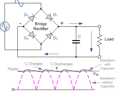
Given Circuit gives a overview on working of full wave
rectifier. A circuit that produces the same output waveform as the full wave
rectifier circuit a is that of the Full Wave Bridge Rectifier. Single phase rectifier uses four
individual rectifying diodes connected in a closed loop bridge configuration to produce the
desired output wave. The advantage of this bridge circuit is that it does not
require a special center tapped transformer, so it reduces its size and cost.
Single secondary winding is connected to one side of the diode bridge network
and the load to the other side.
The four diodes labeled D1 to D4 are arranged in series
pairs with only two diodes conducting current during each half cycle duration.
When the positive half cycle of the supply goes, D1, D2 diodes conduct in a
series while diodes D3 and D4 are reverse biased and the current flows through
the load. During the negative half cycle, D3 and D4 diodes conduct in a series
and diodes D1 and D2 switch off as they are now reverse biased configuration.
THE BASICS OF ELECTRONICS ELECTRONICS.
 Reviewed by Electrotz
on
6:11:00 PM
Rating:
Reviewed by Electrotz
on
6:11:00 PM
Rating:
Reviewed by Electrotz
on
6:11:00 PM
Rating:


No comments: